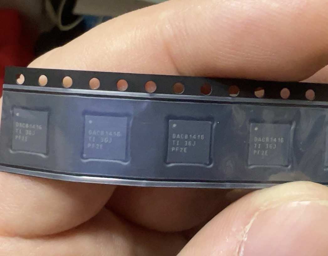
The DAC81416RHAR is a high – performance digital – to – analog converter (DAC) chip with the following key functions:
1. Digital – to – Analog Conversion
• High – Resolution Conversion: It offers a 16 – bit resolution, enabling extremely precise conversion of digital input values into analog output signals. This high resolution allows for the creation of smooth and accurate analog waveforms, making it suitable for applications where fine – grained control of analog signals is crucial, such as in high – end audio systems, precision measurement instruments, and communication test equipment.
• Wide Output Range: The DAC can generate analog output voltages over a specified range. The exact range depends on the power supply configuration and reference voltage settings. It can typically produce output voltages that span a significant portion of the available supply voltage, providing flexibility in meeting the requirements of different analog circuits.
2. Input Interface
• Serial Input: The chip features a serial input interface, which is commonly used to transfer digital data to the DAC. This interface is designed to be compatible with standard serial communication protocols, such as SPI (Serial Peripheral Interface). The SPI – compatible interface allows for easy integration with microcontrollers, DSPs (Digital Signal Processors), and other digital devices. It enables fast and reliable data transfer, with the ability to clock in the 16 – bit digital word in a sequential manner.
3. Reference Voltage
• External Reference Option: The DAC81416RHAR can accept an external reference voltage. The use of an external reference voltage provides greater flexibility in determining the scale and accuracy of the analog output. By choosing a precise external reference voltage source, users can achieve higher levels of accuracy and stability in the analog output. The reference voltage acts as a reference point for the digital – to – analog conversion process, and small variations in the reference voltage can have a direct impact on the accuracy of the output analog signal.
4. Power Management
• Low – Power Operation: It is designed to operate with relatively low power consumption, making it suitable for battery – powered applications or systems where power efficiency is a key consideration. The low – power design helps to extend the battery life in portable devices and reduces the overall power requirements of the system, which is beneficial for applications in which energy conservation is important.
5. Output Buffer
• Buffered Output: The chip often includes an output buffer stage. This buffer provides isolation between the DAC core and the external load, allowing the DAC to drive a variety of load impedances without significant degradation in performance. The output buffer can also improve the output drive capability of the DAC, enabling it to deliver the analog output signal with sufficient current and voltage levels to drive subsequent analog circuits, such as amplifiers or filters.
6. Error Correction and Calibration
• Internal Error Compensation: The DAC81416RHAR may incorporate internal error – correction mechanisms. These mechanisms are designed to minimize the effects of non – idealities in the conversion process, such as gain errors, offset errors, and integral non – linearity (INL). By compensating for these errors, the chip can achieve higher levels of accuracy and linearity in the analog output, ensuring that the output signal closely follows the ideal transfer function from digital input to analog output.









Leave a Reply