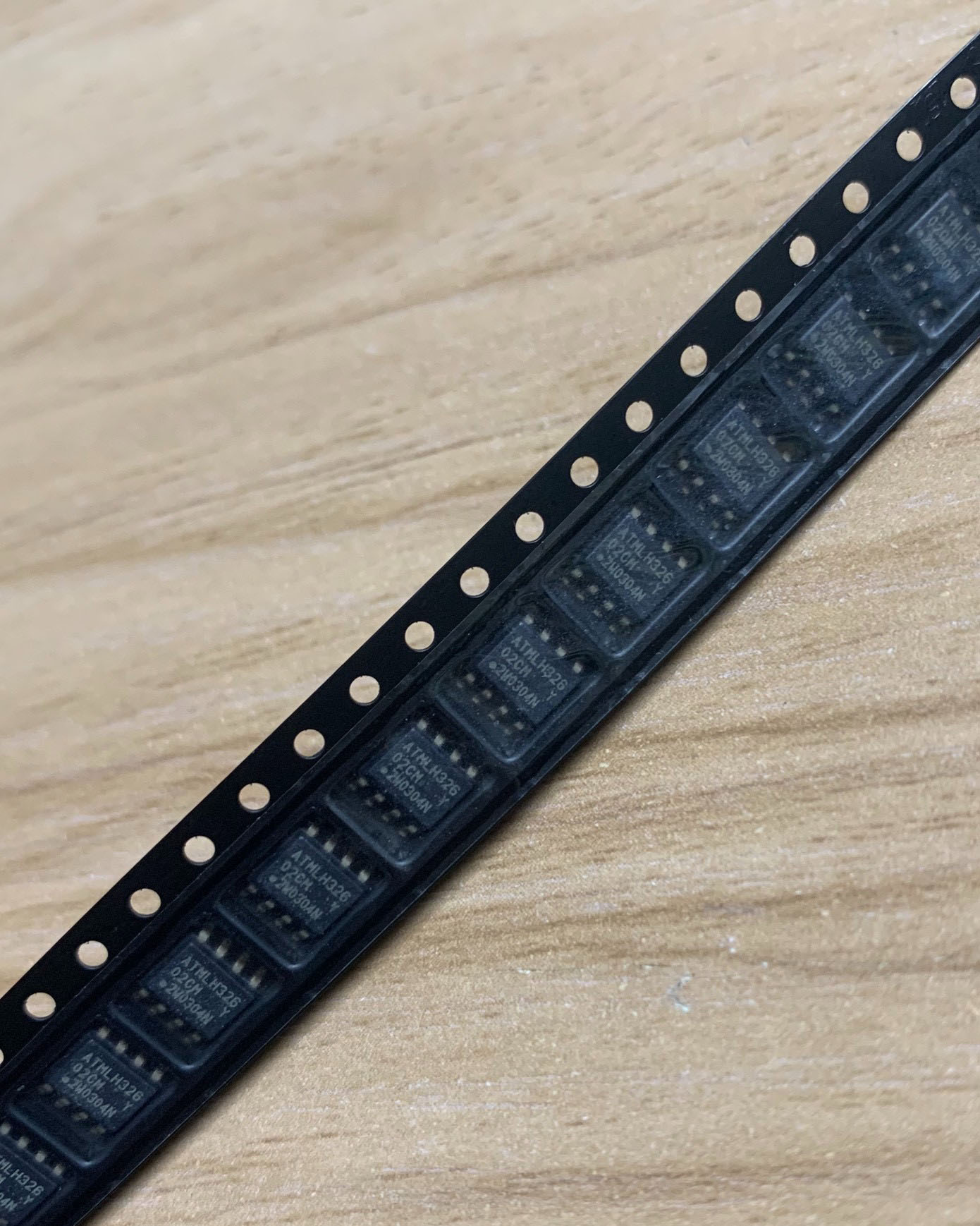
The AT24C02C – SSHM – T is an Electrically Erasable Programmable Read – Only Memory (EEPROM) chip manufactured by Microchip Technology. EEPROMs are non – volatile memory devices, which means they can retain stored data even when the power supply is removed. This particular chip is designed for applications that require reliable data storage and retrieval, such as industrial control systems, consumer electronics, and automotive electronics.
2. Memory Capacity and Organization
2.1 Memory Capacity
- The AT24C02C – SSHM – T has a memory capacity of 2 kilobits (2Kb). This is equivalent to 256 bytes of data storage space. It provides sufficient room to store various types of data, including configuration settings, calibration data, and small – scale user data. For example, in a smart home device, it can store the user – defined settings for the device’s operation, such as temperature thresholds, lighting schedules, etc.
2.2 Memory Organization
- The memory is organized as 256 words of 8 bits each. This byte – organized structure makes it easy to access and manipulate individual bytes of data. Each byte in the memory has a unique address, ranging from 0 to 255. This addressing scheme allows for straightforward read and write operations, where the user can specify the address of the byte they want to access.
3. I²C Interface
3.1 Communication Protocol
- The chip communicates with the host device using the Inter – Integrated Circuit (I²C) protocol. The I²C protocol is a widely used two – wire serial communication protocol that is simple, efficient, and allows multiple devices to be connected to the same bus. The AT24C02C – SSHM – T uses two pins for I²C communication: the Serial Data Line (SDA) and the Serial Clock Line (SCL). The SDA line is used for the transfer of data between the chip and the host, while the SCL line provides the clock signal that synchronizes the data transfer.
3.2 Multiple Device Addressing
- The I²C interface of the AT24C02C – SSHM – T supports multiple device addressing. It has three address pins (A0, A1, A2) that can be used to set the device address. By setting these pins to different logic levels (high or low), up to eight AT24C02C – SSHM – T chips can be connected to the same I²C bus. This feature is useful in applications where multiple EEPROMs are required to store a larger amount of data or in systems where different types of I²C – compatible devices need to co – exist on the same bus.
4. Read and Write Operations
4.1 Byte Read Operation
- To read a single byte of data from the AT24C02C – SSHM – T, the host device first sends a start condition on the I²C bus, followed by the device address and a write bit (logic 0). Then, it sends the address of the byte to be read. After that, the host sends a repeated start condition, followed by the device address and a read bit (logic 1). The chip then sends the requested byte of data on the SDA line, and the host can receive it.
4.2 Byte Write Operation
- For a byte write operation, the host sends a start condition, followed by the device address and a write bit. Then, it sends the address of the byte where the data is to be written, followed by the actual data byte. The chip acknowledges the receipt of each byte. After the data is written, the host sends a stop condition. The AT24C02C – SSHM – T has an internal write cycle time, during which the data is actually programmed into the non – volatile memory cells.
4.3 Page Write Operation
- The chip also supports page write operations. A page in the AT24C02C – SSHM – T consists of 8 bytes. The host can write up to 8 consecutive bytes in a single page write operation. This is more efficient than writing bytes one by one, as it reduces the number of I²C transactions required. To perform a page write, the host follows a similar procedure as the byte write, but it can send up to 8 data bytes in sequence after specifying the starting address of the page.
5. Data Retention and Endurance
5.1 Data Retention
- The AT24C02C – SSHM – T is designed to have a long data – retention period. It can retain the stored data for up to 100 years at a temperature of 25°C. This makes it suitable for applications where the data needs to be stored for a long time without being lost, such as in archival systems or in devices that are installed in remote locations and may not have frequent power cycling.
5.2 Write Endurance
- The chip has a high write endurance. It can withstand up to 1 million write cycles. This means that the data in the memory can be rewritten up to 1 million times without significant degradation. This high write endurance is important in applications where the data needs to be updated frequently, such as in a system that records sensor readings at regular intervals.
6. Power Supply and Operating Conditions
6.1 Power Supply Voltage
- The AT24C02C – SSHM – T operates with a power supply voltage range of 1.8V to 5.5V. This wide voltage range allows it to be used in different types of systems, including low – voltage battery – powered devices and standard 5V – based systems. The chip can automatically adjust its internal operation according to the applied power supply voltage, ensuring reliable performance across the entire voltage range.
6.2 Operating Temperature Range
- It can operate within a temperature range of – 40°C to 85°C. This wide operating temperature range makes it suitable for use in various environments, from industrial settings where the temperature can be extreme to automotive applications where the device may be exposed to high – temperature under – hood conditions or low – temperature cold – start situations.





Leave a Reply