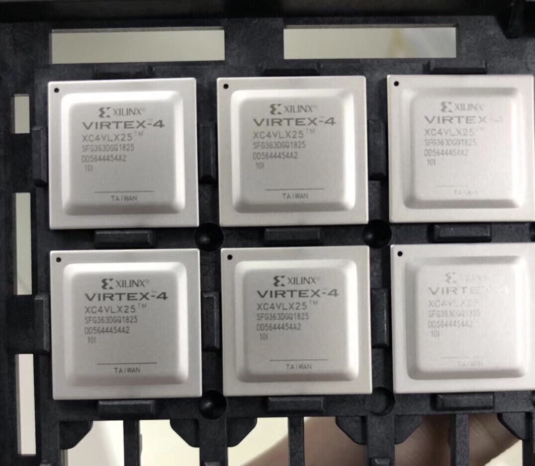
The XC4VLX25 – 10SFG363I is a Field – Programmable Gate Array (FPGA) from the Xilinx Virtex – 4 LX family. Here are its main functions:
1. Programmable Logic
• Logic Cells: It contains a large number of configurable logic blocks (CLBs). These CLBs consist of flip – flops and look – up tables (LUTs). The LUTs can implement any combinational logic function with a certain number of inputs, while flip – flops are used for sequential logic. This allows designers to create a wide variety of digital circuits, from simple logic gates to complex state machines. For example, a designer can use CLBs to build a custom – designed arithmetic logic unit (ALU) for a specific digital signal processing task.
• Interconnect Resources: The FPGA has an extensive interconnect network. This network enables the connection of different CLBs, input/output blocks (IOBs), and other on – chip components. The interconnect is programmable, allowing designers to route signals between different parts of the circuit as required. This flexibility is crucial for creating complex, multi – component digital systems.
2. Digital Signal Processing (DSP)
• DSP Slices: The XC4VLX25 – 10SFG363I includes dedicated DSP slices. These slices are optimized for high – speed digital signal processing operations. They can perform functions such as multiplication, accumulation, and filtering at a high rate. For instance, in a digital communication system, these DSP slices can be used to implement digital filters for signal modulation and demodulation, or to perform fast Fourier transform (FFT) operations for spectral analysis.
3. Input/Output (I/O)
• I/O Blocks: The chip is equipped with multiple I/O blocks (IOBs). These IOBs can be configured to support different I/O standards, such as LVTTL (Low – Voltage Transistor – Transistor Logic), LVCMOS (Low – Voltage Complementary Metal – Oxide – Semiconductor), and differential signaling standards like LVDS (Low – Voltage Differential Signaling). This allows the FPGA to interface with a wide range of external devices, including microcontrollers, memory chips, and communication modules. For example, it can be used to interface with a high – speed serial communication link using the LVDS standard.
4. Memory Resources
• Block RAMs: It contains on – chip block random – access memories (Block RAMs). These Block RAMs can be used for various purposes, such as storing data for digital signal processing algorithms, buffering data in communication systems, or acting as program memories in some custom – designed embedded systems. The Block RAMs can be configured as dual – port RAMs in some cases, enabling concurrent read and write operations, which is useful for applications that require high – speed data access.
5. Configuration and Clocking
• Configuration: The FPGA can be configured with user – defined bitstreams. This is typically done through an external configuration device or a host microcontroller. The configuration process defines the functionality of the FPGA, determining how the logic cells, DSP slices, and other components are interconnected and programmed. The XC4VLX25 – 10SFG363I supports different configuration modes to accommodate different system requirements.
• Clocking: It has a sophisticated clock management system. This includes clock buffers, phase – locked loops (PLLs), and delay – locked loops (DLLs). The clock management system allows for the generation, distribution, and synchronization of clock signals within the FPGA. Different parts of the circuit can be clocked at different frequencies, and the clock signals can be adjusted in terms of phase and duty cycle to meet the timing requirements of various digital circuits.




Leave a Reply