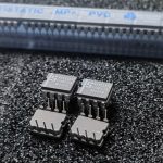
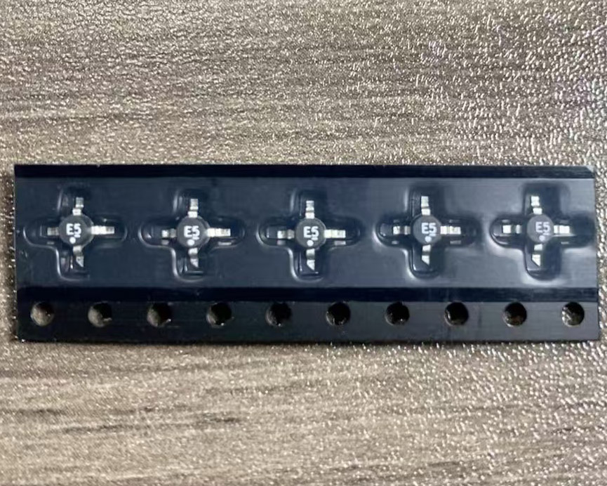
The AT24C02C chip is a 2Kb serial EEPROM, and its functions are briefly described as follows: – Data Storage Function: It has an internal storage space of 256 8-bit bytes, organized as 256×8. It can store a small amount of critical data, such as configuration parameters and calibration data.
– Communication Interface Function: It adopts the I2C serial bus interface and only requires two wires, namely serial data (SDA) and serial clock (SCL), to communicate with the master device. It supports two-way data transmission and can be easily connected to master devices such as single-chip microcomputers to achieve data reading and writing operations.
– Write Protection Function: It is equipped with a dedicated write protection pin WP. When the WP pin is connected to a high level (VCC), the data in the chip is protected and only read operations are allowed, preventing the data from being accidentally overwritten. When it is connected to a low level (GND) or left floating, normal read/write operations are allowed.
– Flexible Addressing Function: The device address can be set through the A0, A1, and A2 pins. Up to 8 AT24C02C chips can be connected to the same I2C bus. Device selection can be carried out through different configurations, enabling the cascaded use of multiple chips.
– Low Power Consumption Function: It adopts advanced CMOS technology, with an operating current as low as 1mA and a standby current as low as 1μA or 6μA, making it suitable for low-power application scenarios with strict power consumption requirements.
– High Reliability Function: It has up to 1 million erase/write cycles and a data retention time of over 100 years. It also has Schmitt trigger input filtering to suppress noise and ensure the stability and reliability of data storage and transmission.
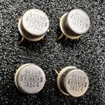