1. Latching Function
Data Storage: The 74HC573D is designed to latch (store) 8 – bits of digital data. When enabled in the appropriate mode, it can capture and hold the input data levels. This is useful in digital systems where data needs to be temporarily stored or synchronized. For example, in a microcontroller – based system, it can be used to store the output data from the microcontroller for a short period until it is ready to be transferred to other components such as a display driver or a peripheral device.
Transparent Latch Mode: It operates in a transparent latch mode. In this mode, as long as the latch enable (LE) input is in a particular state (usually high), the output follows the input. That is, the data at the output ports is the same as the data at the input ports. When the LE input changes to the opposite state (usually low), the data present at the inputs at that moment is latched and the outputs remain at those values until the LE input changes again to the transparent state.
2. Tri – State Outputs
Output Control: The device has tri – state outputs. This means that the output pins can be put into a high – impedance state. A separate output enable (OE) input controls the output state. When the OE input is in a particular state (usually low), the outputs are enabled and the latched data is presented at the output pins. When the OE input is in the opposite state (usually high), the output pins go into a high – impedance state. This allows multiple devices to be connected to a common bus without interfering with each other. For example, in a shared – data – bus architecture, the high – impedance state of the outputs of the 74HC573D can be used to disconnect its data from the bus when it is not its turn to transfer data.
3. Electrical Characteristics
High – Speed Operation: The 74HC573D is a high – speed CMOS device. It can operate at relatively high frequencies, enabling fast data transfer and latching operations. The propagation delay from the input to the output (when the latch is transparent) and the setup and hold times for latching the data are relatively short, which is beneficial for applications that require quick response times, such as in digital communication systems or high – speed data acquisition setups.
Wide Operating Voltage Range: It has a wide operating voltage range. Typically, it can operate with a supply voltage (VCC) ranging from 2V to 6V. This flexibility in voltage supply allows it to be used in a variety of power – supplied digital systems, from battery – powered portable devices to systems with more stable power supplies.
4. Package and Compatibility
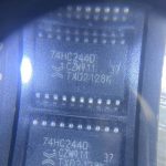
DIP and SMT Packages: The 74HC573D is available in different package types, such as Dual In – Line Package (DIP) and Surface Mount Technology (SMT) packages. The DIP package is convenient for prototyping and through – hole mounting on printed circuit boards, while the SMT packages are suitable for high – volume manufacturing and more compact circuit designs.
Logic Compatibility: It is compatible with other standard TTL (Transistor – Transistor Logic) and CMOS (Complementary Metal – Oxide – Semiconductor) logic families. This makes it easy to interface with a wide range of other digital components such as microcontrollers, logic gates, decoders, and multiplexers in a digital circuit design.


